GaN devices will see explosive growth in the 5G era
The RF power amplifier (PA) is the main component of the RF front-end transmit path and is typically used to amplify the RF signal of the transmit channel. 5G will drive the smart mobile terminal, base station and IOT equipment RF PA to grow steadily. The mobile radio terminal RF PA market will grow from US$5 billion in 2017 to US$7 billion in 2023, with a compound annual growth rate of 7% and high-end. The growth of the LTE power amplifier market, especially high frequency and ultra high frequency, will make up for the shrinking of the 2G/3G market. GaAs devices are the main force in consumer electronics 3G/4G applications, and the 5G era will continue. In addition, the Internet of Things will be the blue ocean for its future applications. GaN devices are widely used in military fields such as base stations, radars, and electronic warfare with high performance characteristics. In the 5G era, demand will usher in explosive growth.
In 5G base stations, PA has increased several times, and GaN has a lot to offer.
4G base station adopts 4T4R scheme, according to three sectors, the corresponding RF PA demand is 12, 5G base station, 64T64R is expected to become the mainstream solution, the corresponding PA demand is up to 192, and the number of PA will increase significantly. At present, power amplifiers for base stations are mainly LDMOS technologies, but LDMOS technology is suitable for low frequency bands and has limitations in the field of high applications. The 5G base station GaN RF PA will become the mainstream technology, gradually occupying the LDMOS market, and the GaAs device share will not change much. GaN is better suited for large-scale MIMO. According to Yole’s prediction, the market size of GaN RF in base stations will reach 520 million US dollars in 2023, with a compound annual growth rate of 22.8%.
As far as the telecom market is concerned, thanks to the approaching 5G network application, it will bring huge market opportunities for GaN devices from 2019. Compared to existing silicon LDMOS (transverse double diffused metal oxide semiconductor technology) and GaAs (GaAs) solutions, GaN devices can provide the power and performance required for next-generation high-frequency telecommunications networks. Moreover, the broadband performance of GaN is also one of the key factors in achieving important new technologies such as multi-frequency carrier aggregation. GaN HEMTs (High Electron Mobility Field Effect Transistors) have become candidates for future macro base station power amplifiers.
For a given power level, GaN has the advantage of being small in size. With smaller devices, device capacitance can be reduced, making the design of higher bandwidth systems easier.
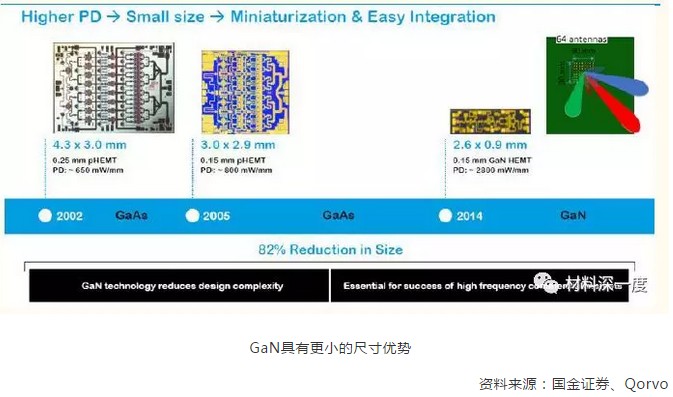
GaN has a smaller size advantage
Source: Guojin Securities, Qorvo
Since LDMOS cannot support higher frequencies, GaAs is no longer the optimal solution for high-power applications. It is expected that most of the macro network unit applications below 6 GHz will use GaN devices in the future, but the advantages of GaAs in small base stations are more obvious. The 5G network uses a higher frequency band, and the penetration and coverage will be worse than 4G. Therefore, the small cell will play a very important role in the 5G network construction. However, since small base stations do not require such high power, the prior art such as GaAs still has its advantages. At the same time, as higher frequencies reduce the coverage of each base station, more transistors need to be applied, and market shipment growth is expected to accelerate.
GaN is suitable for massive MIMO
GaN chips will make a leap in power density and packaging every year, and are better suited for large-scale MIMO technology. Current base station technology involves a MIMO configuration with up to 8 antennas to control the signal by a simple beamforming algorithm, but massive MIMO may require hundreds of antennas to achieve the data rate and spectral efficiency required for 5G. The power-hungry active electronically scanned array (AESA) used in mass MIMO requires a separate PA to drive each antenna element, which brings significant size, weight, power density, and cost (SWaP-C) challenge. This will always involve RF PAs that are capable of meeting 64 components and beyond the power, linearity, thermal management and size requirements of the MIMO array with minimal deviation on each transmit/receive (T/R) module.
GaN-on-SiC has advantages
There are still two technologies competing on the market: GaN-on-SiC (gallium nitride on silicon carbide) and GaN-on-silicon (gallium nitride on silicon). They use substrates of different materials but have similar properties. In theory, GaN-on-SiC has better performance, and most manufacturers currently adopt this technical solution. However, manufacturers such as MACOM are pushing the widespread use of GaN-on-Silicon technology. It is too early to say who will dominate in the future. At present, GaN-on-silicon is still a strong challenger for GaN-on-SiC solutions.
The development direction of the GaN RF market
GaN manufacturing is mainly based on IDM. After decades of development, GaN technology has become popular on all continents. Market-leading vendors include Sumitomo Electric, Wolfspeed (Cree), Qorvo, and many other vendors in the US, Europe and Asia. The compound semiconductor market is different from the traditional silicon-based semiconductor industry. Compared with the traditional silicon process, the epitaxial process of GaN technology is much more important, which will affect the quality of its active region and have a huge impact on the reliability of the device. This is why the current market-leading manufacturers have strong epitaxial process capabilities, and in order to maintain technical secrets, they tend to put these processes in their own internal production. Despite this, Fabless design vendors are growing fast through collaboration with foundry partners. Leading vendors such as NXP and Ampleon may change the competitive landscape in the market due to close partnerships with the foundries and sales channels.
The above sharing information comes from the Internet, and the copyright and opinions belong to the original author. |


 Sale.
Sale.